RTL Design
Digital architecture and RTL implementation in VHDL and Verilog, structured around the throughput and latency the system actually demands rather than what is convenient to write.
VHDLVerilogArchitecture

A&W Engineering Works provides FPGA and ASIC design services across India from our engineering office in Vadodara, Gujarat. We cover HDL design, verification, and GPU-based high-performance computing for demanding real-time and data-intensive workloads — the digital hardware that has to keep pace with a sensor in real time, verified to the standard a medical device programme requires.
Digital architecture and RTL implementation in VHDL and Verilog, structured around the throughput and latency the system actually demands rather than what is convenient to write.
Testbenches, coverage and bit-exact reference models used to prove the hardware matches the algorithm it came from. Verification is a discipline we recruit for, not an afterthought.
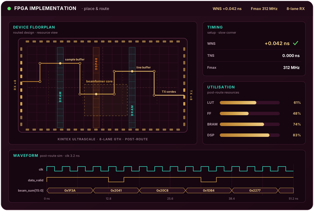
Processing pipelines implemented in fabric where software cannot keep up, including real-time transmit and receive beamforming for high frame rates and image quality.
Timing closure, resource and power optimisation, and the architectural trade-offs that decide whether a design fits the part you chose or forces you onto a larger one.
GPU-based high-performance computing for data-intensive workloads that belong off the FPGA — reconstruction, offline processing, and anything adjacent to machine learning.
An FPGA is one block in a chain. We connect it to the processor sub-system, embedded software, the analog front end and the sensors, and make the whole path testable.
Hardware implementing an algorithm should be provably equivalent to that algorithm. We work from the model down, so what runs in fabric can be checked against a reference at every stage instead of being debugged on a board.
What leaves our office at the end of a piece of FPGA work. The exact set depends on scope, and we agree it in writing before starting rather than at handover.
Our engineering team works from two hubs: an engineering office in Vadodara, Gujarat and headquarters in Silicon Valley. Most day-to-day design and verification work is carried out by the Vadodara team, which means clients across India — in Bangalore, Hyderabad, Pune, Delhi NCR, Ahmedabad and beyond — get direct access to the engineers doing the work, in the same time zone, at competitive rates — while the US office keeps the programme close to customers in North America.
India — Engineering Office: 301-306 (3rd Floor), Ozone, Sarabhai Road, Vadodara, Gujarat 390023 ·
+91 265 3100926 ·
contact@awengworks.in
USA — Headquarters: 1307 S. Mary Ave., Suite 260, Sunnyvale, CA 94087
Both. We are often engaged for a self-contained HDL block or a verification effort inside someone else's programme, and equally often for the digital architecture of an entire system. Tell us the boundary you want us to work inside and we will scope to it.
VHDL and Verilog for RTL, with the vendor toolchain your target device requires. We also build GPU-based high-performance computing where a workload belongs off the FPGA.
Yes. Our normal flow starts from a floating-point algorithm model, derives a bit-exact reference, implements RTL against it, and verifies with testbenches and coverage — so the finished hardware can be shown to match the algorithm it came from.
In our engineering office at Ozone, Sarabhai Road, Vadodara, Gujarat, with company headquarters in Sunnyvale, California. Clients across India work directly with the Vadodara team.
Whether it is one HDL block, a verification effort, or the digital architecture for a whole product, tell us the constraints and we will tell you honestly what we would do.