Enclosure & Housing Design
Product enclosures designed around the board, the display, the connectors and the human hand — not a box the electronics have to be forced into afterwards.
3D CADIndustrial designErgonomics

Enclosures, housings and mechanical assemblies for electronic products — designed together with the electronics inside them, not around them. From 3D CAD and thermal strategy through design for manufacture, with in-house rapid prototyping to close the loop between drawing and part.
Product enclosures designed around the board, the display, the connectors and the human hand — not a box the electronics have to be forced into afterwards.
Heat paths, vents, spreaders and sinks decided early, from the electronics' real power budget — because a thermal problem found at the prototype stage is a mechanical redesign.
Parts designed for the process that will actually make them — injection moulding, sheet metal or machining — with draft, wall thickness, tolerances and assembly order thought through.
Stack-up analysis, fits and datum schemes agreed before parts are cut, so assemblies go together the same way at unit one and unit ten thousand.
Housings for transducers, probes and sensors — where acoustic coupling, sealing, cable strain relief and cleaning requirements matter as much as the outside surface.
In-house 3D printing and quick-turn parts to test fit, feel and assembly in days — so the design that goes to tooling has already been held, dropped and taken apart.
An enclosure is the last thing a user forgives and the first thing they touch. We design it from the inside out — the board, the heat, the connectors — and from the outside in — the grip, the workflow, the look — at the same time.
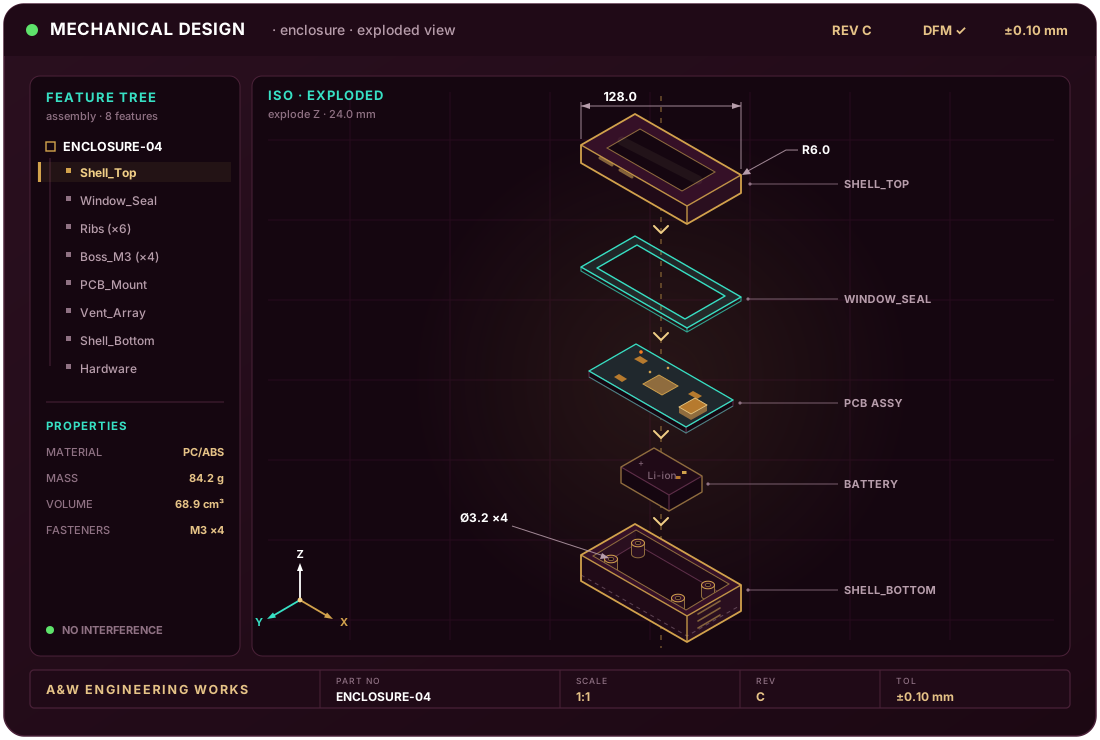
What leaves our office at the end of a piece of mechanical work. The exact set depends on scope, and we agree it in writing before starting rather than at handover.
Our engineering team works from two hubs: an engineering office in Vadodara, Gujarat and headquarters in Silicon Valley. Most day-to-day design work is carried out by the Vadodara team, which means clients across India — in Bangalore, Hyderabad, Pune, Delhi NCR, Ahmedabad and beyond — get direct access to the engineers doing the work, in the same time zone, at competitive rates — while the US office keeps the programme close to customers in North America.
India — Engineering Office: 301-306 (3rd Floor), Ozone, Sarabhai Road, Vadodara, Gujarat 390023 ·
+91 265 3100926 ·
contact@awengworks.in
USA — Headquarters: 1307 S. Mary Ave., Suite 260, Sunnyvale, CA 94087
Both. Most engagements pair mechanical design with our hardware and systems teams, which is where the approach pays off most — but we also take on standalone enclosure, thermal and DFM work for boards designed elsewhere.
Injection moulding, sheet metal and machining for production, and 3D printing for prototypes and low volumes. We design for the process your volumes and budget actually justify, and review the design with the manufacturer before release.
Yes. We 3D print in-house and use quick-turn suppliers for parts we cannot print, so fit, feel and assembly get tested in days rather than weeks. See our rapid prototyping page for how we work.
In our engineering office at Ozone, Sarabhai Road, Vadodara, Gujarat, with company headquarters in Sunnyvale, California. Clients across India work directly with the Vadodara team.
Whether it is a handheld device, a probe housing or a rack instrument, tell us the constraints and we will tell you honestly how we would design it — and what it will take to manufacture.