Schematic Capture
Schematic design worked out from the system requirements — component selection, interfaces and margins decided deliberately, and documented so the reasoning survives past the first review.
SchematicsPart selectionReviews

Electronic hardware design from our Vadodara engineering office — schematic capture, PCB layout, mixed-signal and power design, and the sensor and connector integration that turns a block diagram into a board you can build. We design hardware as part of a whole system rather than in isolation, which is why our boards arrive with the software and signal chain already accounted for.
Schematic design worked out from the system requirements — component selection, interfaces and margins decided deliberately, and documented so the reasoning survives past the first review.
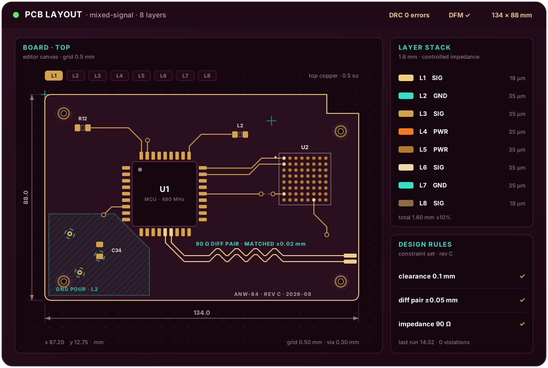
Multi-layer layout carried out with signal integrity in mind from the first placement, not corrected afterwards — stack-up, impedance control, return paths and length matching where they matter.
The boundary where analog and digital coexist: supply and reference design, grounding and partitioning, and keeping switching noise out of sensitive receive paths.
Sensor systems and data-control integration — connecting transducers, electronics and software into reliable, testable products rather than a set of working sub-assemblies.
Manufacturability and test access treated as requirements from the start: test points, programming and bring-up headers, tolerance and assembly considerations.
Getting the first boards alive and characterised — power sequencing, clocking, interface validation, and the measurements that confirm the design meets its budget.
Most expensive hardware problems are decided early and discovered late. Our process front-loads the decisions that force a respin if they are wrong, and defers the ones that do not.
A hardware package should let another team manufacture and maintain the board without needing us. The exact list is agreed at the start of the engagement.
Our engineering team works from two hubs: an engineering office in Vadodara, Gujarat and headquarters in Silicon Valley. Most day-to-day design and verification work is carried out by the Vadodara team, which means clients across India — in Bangalore, Hyderabad, Pune, Delhi NCR, Ahmedabad and beyond — get direct access to the engineers doing the work, in the same time zone, at competitive rates — while the US office keeps the programme close to customers in North America.
India — Engineering Office: 301-306 (3rd Floor), Ozone, Sarabhai Road, Vadodara, Gujarat 390023 ·
+91 265 3100926 ·
contact@awengworks.in
USA — Headquarters: 1307 S. Mary Ave., Suite 260, Sunnyvale, CA 94087
Yes. We are engaged both for standalone schematic capture and PCB layout, and for complete hardware programmes where we also handle the analog front end, embedded software and system integration.
Yes — medical devices are our main domain. We work with an understanding of ISO 13485, QMS, FDA expectations, risk analysis and documentation, and the design trade-offs that come with them.
We deliver a complete manufacturing pack — Gerbers, drill files, pick-and-place, bill of materials and assembly notes — designed so your chosen manufacturer can build it. We support bring-up and characterisation of the first boards.
Our engineering office is at Ozone, Sarabhai Road, Vadodara, Gujarat 390023, with headquarters in Sunnyvale, California.
From a single PCB to the full electronics for a product, tell us what it has to do and we will tell you what it takes.